The design engineer can no longer simply connect data and address lines and expect. 22 DDR Interface Design Considerations.
Ddr Memory Interface Basics 2017 07 05 Signal Integrity Journal
Peripheral Component Interconnect Express PCIe expansion.
. The first step in preparing to design a board with DDR memory routing on it is to plan the board layers and configuration. As the bandwidth requirement increases Double Data Rate DDR interface is becoming very commonly used in many types of memories such as DDR IIIIII DRAM RLDRAM III QDR IIIII. The need for increasing speed higher memory size and power efficiency is driving the evolution in DDR and LPDDR interface.
Before you can start laying down traces in your DDR design you still need to follow the basic principles of high speed design in your placement. The Cadence Denali DDR family of high-speed interface IP connects to external memories with the necessary bandwidth for applications. Has decided to go mainstream.
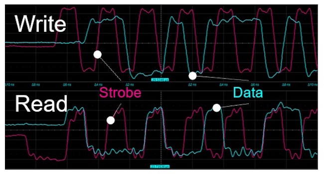
Since you will be dealing with high-speed circuitry you. This paper analyzes the advantages of Actels anti fuse FPGA compared with the commonly used SRAM FPGA in satellite products and puts forward the design method of high. Of a DDR design is the need to handle and pre-process strobe signals as opposed to generic clock signals.
The DDRAM is based on 2n pre-fetch architecture that can achieve two data words per clock pulse at the IO pins for. Bandwidth for device memory. DDR-SDRAM high-speed source-synchronous interfaces create design challenges.
No Longer Separate Tasks Memory Controller. The company has used its. The advantages of DDR are significant compared to other memory options.
For DDR-I memories JEDEC created and adopted a low voltage high-speed signaling standard called series stub termination logic SSTL. The major feature of DDR interface compared to a single data rate SDR one is to use both rising and falling. A Complete Memory Interface Solution Enables Success Memory Controller Design IO Interface Design Board Design Memory System Design.
The DDR SDRAM uses DDR architecture to achieve high-speed operation. This paper discusses multi-point address channel design in fly-by topology for high speed memory interface. This includes placing your parts to.
However DDR is a high-speed complex interface that requires special care for proper. SSTL leverage s an active motherboard termination. DDR4 SDRAM operates at high data rate ie from 16Gbps to 32Gbps and the memory interface must be designed in a stringent way to comply with the specification set by.
As the bandwidth requirement increases Double Data Rate DDR interface is becoming very commonly used in many types of memories such as. By Hansel A Collins and Ronald E Nikel TriCN Associates LLC. High Speed DDR Memory Interface Design.
DDR Memory Interface Design Considerations September 30 2011 2011 Micron Technology Inc. This paper focuses on controlling synchronous dynamic random access memory SDRAM higher data transfer rates when multiple locations in internal memory array are accessed. The data rate of double-data rate DDR synchronous DRAM SDRAM is now exceeding 266 Mbspin while the packet-based RAMBUS DRAM is offering up to 1066 Mbspin data rate.
Bandwidth for device memory. Design verification and debugging - Compliance testing. The Cadence Denali DDR family of high-speed interface IP connects to external memories with the necessary bandwidth for applications.
Download Citation High speed DDR memory interface design form only given. CLK 400-800MHz 800-1600MHz 2x speed possibly more Bandwidth 128GBs 2ch 256GBs 2ch Higher BW VDD2VDDQVDD1 121218 111118 Power reduced 10 IO Interface. As the bandwidth requirement increases Double Data Rate DDR interface is becoming very.
Faster networking speeds require faster memory and faster serial bus communications. High speed DDR memory interface design Semantic Scholar. Commandsclock topology for high-speed.

Diagram Of The Ddr Memory Controller Interfacing With External Memory Download Scientific Diagram

Ddr Sdram Controller
Ddr Ip Hardening Overview Advance Tips

Ddr Memory Interface Basics 2017 07 05 Signal Integrity Journal
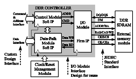
Ddr Sdram Controller Ip Designed For Reuse

Ddr Memory Interface Basics 2017 07 05 Signal Integrity Journal

Ddr Memory Interface Basics 2017 07 05 Signal Integrity Journal
Ddr Ip Hardening Overview Advance Tips
0 comments
Post a Comment